Thermal Imaging at the Microscale
Accurate thermal failure analysis detection has become increasingly difficult because of shrinking semiconductor devices and rising power density. Localized heating often indicates defects such as leakage current, short circuits, resistive failures, and stressed components. Left undetected, hotspots can lead to performance degradation, reduced reliability, or device failure.
Accurate hotspot detection is complicated by several factors, particularly when dealing with advanced ICs, where defects may be buried beneath multiple layers or deep within silicon substrate. Key challenges include:
- Limited spatial resolution
- Low or inconsistent emissivity
- Device packaging and metal layers
- Access constraints, particularly for backside analysis
- Very low power dissipation
These constrains make the choice of imaging wavelength and technique crucial. The differences between mid-wave infrared (MWIR) and long-wave infrared (LWIR) imaging significantly impact defect detectability and fault localization--particularly when comparing frontside and backside analysis.
MWIR vs LWIR Imaging -- Key Differences
The main difference between MWIR and LWIR imaging is the wavelength range they detect, which directly affects how they interact with materials, their resolution, and their suitability for different applications.
Below is a breakdown of the differences between MWIR and LWIR imaging:
| Feature | MWIR | LWIR |
Wavelength | ~3–5 µm (mid-wave infrared) | ~8–12 µm (long-wave infrared) |
Spatial resolution | Finer (shorter wavelengths enable finer spatial detail) | Courser (longer wavelength limit) |
Thermal sensitivity (NETD) | NETD 15-30 mK (Higher sensitivity, typically with cooled detectors) | NETD 40-50 mK (reduced sensitivity to subtle thermal variations) |
Transmission through silicon | Partial transmission through silicon | Opaque to silicon (mostly measures surface emission) |
| Emissivity dependence | Less sensitive to emissivity variation | Highly dependent on surface emissivity |
Cost | Higher (typically cooled systems) | Lower (often uncooled systems) |
Best suited for | IC failure analysis, backside imaging, microscale defect localization | Large and small PCB inspection, surface thermal mapping |
Frontside vs Backside Thermal Imaging
Imaging strategy depends heavily on the depth of the defective features. In frontside analysis, active structures are closer to the surface and more readily observable. In contrast, backside analysis involves imaging through the silicon substrate, requiring shorter wavelengths, where silicon becomes transparent.
LWIR imaging is generally ineffective for backside analysis because the silicon is largely opaque in this wavelength range. As a result, the silicon substrate must be completely removed to expose active layers.
MWIR imaging, however, enables detection of thermal signatures through the substrate, reducing destruction of the deice, and enabling faster, less invasive analysis.
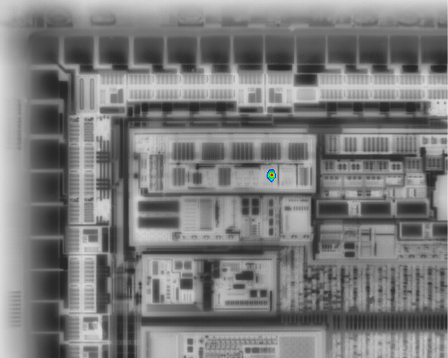
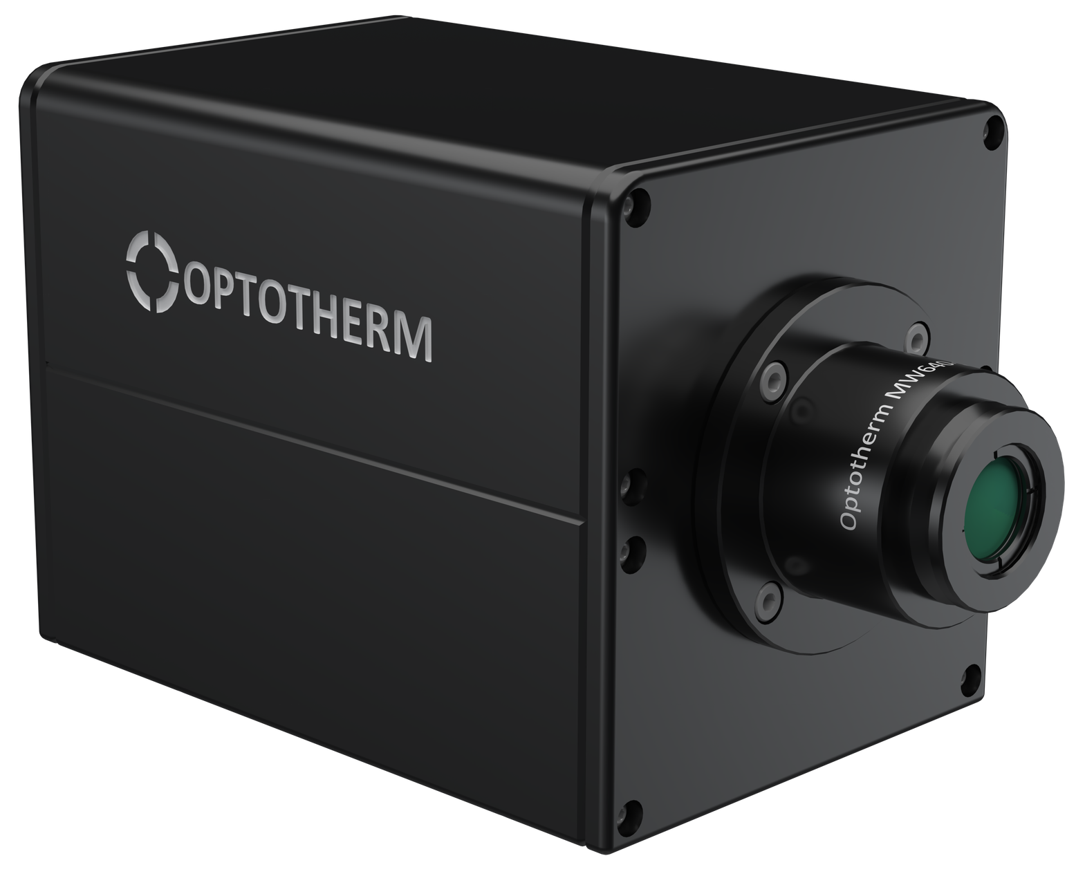
MWIR imaging is commonly used in high-resolution IC and PCB failure analysis systems. For example, a Sentris system equipped with the MW640-15 camera from Optotherm, Inc. is capable of resolving features down to approximately 1 μm, enabling precise localization of thermal anomalies at the microscale.
When to Use MWIR vs LWIR
Use MWIR in applications including:
- Backside imaging through silicon
- High-resolution defect localization
- Low emissivity surfaces
Use LWIR in applications including:
- Large-scale thermal mapping
- Cost-sensitive setups
- General PCB / board-level analysis
Key Takeaways:
- MWIR imaging provides the spatial resolution and deep material detection needed for advanced semiconductor failure analysis.
- LWIR imaging remains useful for surface-level thermal imaging and larger-scale applications.
- MWIR imaging enables backside failure analysis through silicon due to its partial transparency in the 3–5 µm wavelength range.
- LWIR imaging is limited in its ability to resolve fine features or image through semiconductor substrates.