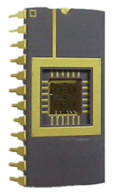
Thermal Test Chip
PN0308 contains several heat-generating elements including two deposited metal film resistors and four diodes. Voltage can be applied to the resistors or diodes to heat each element.
Applications
-
Train system users to perform tests such as lock-in thermography.
Overview
Resistors
The resistor on the left of the die (see Figure 2) can be heated by applying a DC voltage across pins 4 and 21 as shown in the pin-out in Figure 1. Likewise, the resistor on the right of the die can be powered by applying voltage across pins 9 and 16. Resistors have resistance of 7.6 ohm ± 10% and have a low resistance temperature coefficient of approximately 20 ppm/°C, resulting in relatively constant power dissipation during thermal measurements. The design recommended maximum current handling capacity of each resistor, connection trace, and pad is 0.89 A, allowing each resistor to dissipate up to 6 W. Apply 1 V across a resistor will result in power dissipation of approximately 132 mW. To decrease power dissipation (and therefore reduce the temperature) of the resistor, decrease the applied voltage.
Caution: Current should be limited to a maximum of 0.89 A when applying voltage across a resistor to prevent damage to the Thermal Test Chip.
Diodes
Diode D1 in the top right of the die (see Figure 2) can be forward biased by applying a +VDC to pin 15 with respect to pin 14. Diode D2, D7, and D8 can be forward biased by applying a +VDC to the appropriate pins. Each diode has nominal VF of 0.71 V @ IF = 1 mA and nominal BVR ≥ 5 V @ IR = 10 µA. Because the forward resistance of the diode is very low, the power supply current must be limited to a maximum of 10 mA. The diode has a forward voltage drop of approximately 0.71 V, thus applying +1 V to pins 13 (with respect to pin 6) will result in power dissipation in the diode of approximately 7.1 mW if the current is limited to 10 mA. To decrease power dissipation (and therefore reduce the temperature) of the diode, reduce the current below 10 mA.
Caution: When a diode is forward-biased with a voltage greater than VF, the diode forward resistance is very low, and the power supply current must be limited to a maximum of 10 mA to prevent diode damage.
Included Components
-
2.5 x 2.5 mm silicon semiconductor die enclosed in a 15.24 x 31.5 mm ceramic 24 pin DIP package
Required Products
Related Products
Manufacturer Information
Specifications
Package
| Die Size |
2.5 x 2.5 mm |
| Package |
15.24 x 31.5 mm ceramic 24 pin DIP package |
| Package Pin Pitch | 0.10” (2.54 mm) |
Resistor
| Resistance (each resistor) |
7.6 ohm ± 10% |
| Temperature Coefficient |
Approximately 20 ppm/°C |
| Max Current (each resistor) |
0.89 A |
| Max Power (each resistor) |
6 W |
Diode
| Nominal VF (Forward Voltage Drop) |
0.71 V @ IF = 1 mA |
| Nominal BVR (Breakdown Voltage) |
≥ 5 V @ IR = 10 µA |
| Max Forward Current |
10 mA |
| Forward Voltage Drop |
Approximately 0.71 V |
Setup
Installation
Mounting the Chip
To perform software test on the Thermal Test Chip such as lock-in thermography, the chip must be mounted on the Thermoelectric Vacuum Stage. An aluminum heat sink bar is supplied with the Thermal Test Chip to provide thermal coupling between the Thermoelectric Vacuum Stage and the chip package. The surface of the bar is electrically insulated with hard-coat black anodize to prevent a short-circuit between package pins and test clips. Secure the chip and heat sink bar to the Thermoelectric Vacuum Stage using two Device Spring Clamps (see Figure 1).
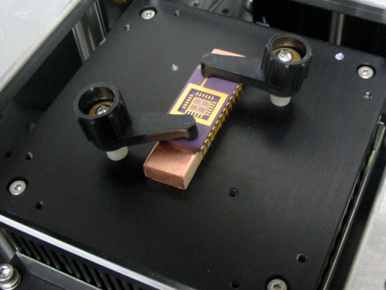
Figure 1: Thermal Test Chip mounted on the Thermoelectric Vacuum Stage
Package Pinout
The thermal test die pins (top view of package) are numbered as shown in Figure 2.
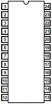
Figure 2: DIP pin numbers (top view)
The internal wire bond connections between the die pads and package pins are shown in Figure 3. Note that the die in the DIP package in Figure 1 is oriented 90° clockwise compared with the die pictured in Figure 3.
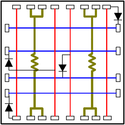
Figure 3: Thermal test die 2x2 array
Operation
Electrical Connections
When performing a lock-in test, voltage to the Thermal Test Chip can be controlled using one of the relays in the relay device or by controlling a Keithley instrument directly. The following instructions explain how to make electrical connections to the resistor on the left of the die using spring clips, High Current Relays, and a voltage source. Electrical connections to the High Frequency Relays are similar, but in this case only two screw terminals (common and normally open) are available.
Resistor Electrical Connections
-
Connect the red banana jack to the positive (+) terminal on the voltage source (see Figure 4).
-
Insert the other end of the red test lead into one of the even-numbered screw terminals (such as contact 0) on the relay and tighten.
-
Connect the red test clip to pin 21.
-
Insert the other end of the red test lead into the next higher-numbered screw terminal (such as contact 1) and tighten.
-
Connect the black banana jack to the negative (-) terminal on the voltage source.
-
Connect the black test clip to pin 4.
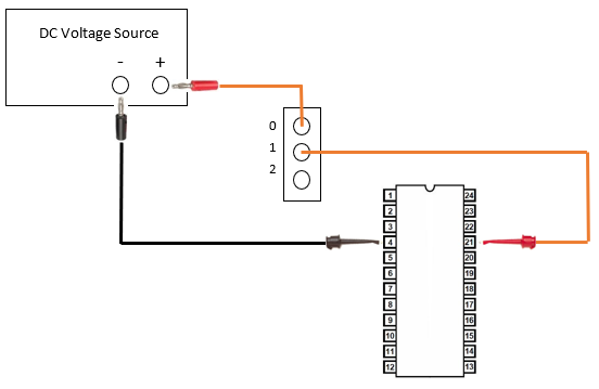
Figure 4: Electrical connections to the resistors on the left of the die
Diode Electrical Connections
-
Connect the red banana jack to the positive (+) terminal on the voltage source supply (see Figure 5).
-
Insert the other end of the red test lead into one of the even-numbered screw terminals (such as contact 0) on the relay and tighten.
-
Connect the red test clip to pin 15.
-
Insert the other end of the red test lead into the next higher-numbered screw terminal (such as contact 1) and tighten.
-
Connect the black banana jack to the negative (-) terminal on the voltage source.
-
Connect the black test clip to pin 14.
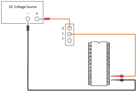
Figure 5: Electrical connections to the Thermal Test Chip diode D1
Troubleshoot
Maintenance