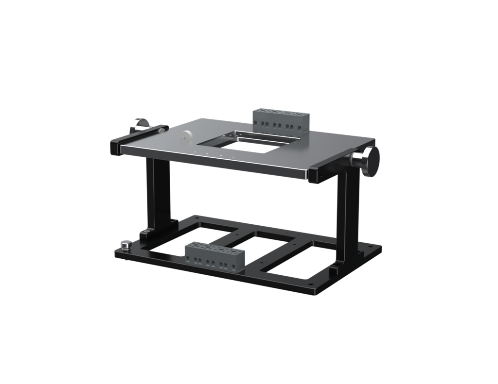
Overview
Used to probe a device or wafer and flip to image the opposite side. Devices are mounted in magnetic chucks made of non-conductive Delrin. Terminal blocks manage voltage source and probe lead connections so the platform can flip upside down. The platform accommodates devices up to 80 mm wide.
Applications
- Flip chip ball grid array analysis
- Backside analysis
Specifications
| Net weight | 6.4kg |
| Dimensions | 35.5 x 20 x 18cm |
| Maximum device size (for die holders) | 80 x 80mm |
Setup, Operation, & Maintenance
Additional product resources are linked under Documents at the bottom of this webpage.
Troubleshooting
Click the link below to view the Support Forum posts for this topic.
[Insert link here]