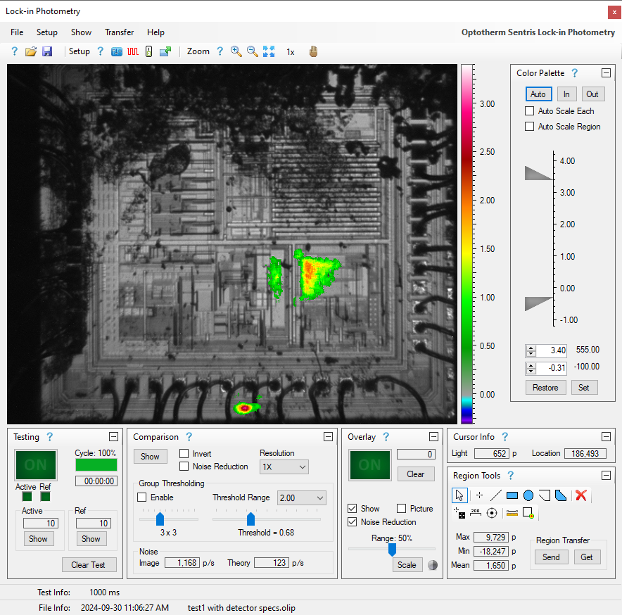
Lock-in Photometry Software Module

https://www.optotherm.com/web/image/product.template/2152/image_1920?unique=d256276

-Description-
Non-destructive (NDT) tool similar to Emission Microscopy (EMMI) and Photon Emission Microscopy (PEM) and is used to detect and locate faults on semiconductor devices by detecting emitted photons in the short-wave infrared (SWIR) region of the electromagnetic spectrum.

-More Information-
Product Information: https://www.optotherm.com/shop/2152


*Lock-in Photometry requires an instrument to perform device bias. Device bias is typically accomplished by connecting the output of a power supply or source meter to exposed leads or pins of package devices or circuit boards, or by landing probes on bare semiconductor devices or circuit boards. A number of Keithley instruments can be directly controlled by Thermalyze software during LIP tests to cycle bias on and off. Refer to the Thermalyze.chm Help file for a list of supported Keithley instruments. *


Internal Reference: PN0896

Explore this product

Overview

Lock-in photometry is a test process comparing the emissions of a biased device to the emissions of an optical shutter (or an unbiased device). The following description is oversimplified but helps to provide a basic understanding of the lock-in process. Over many cycles, captured images of the biased device (Active Images) are added together.  Likewise, captured images of the unbiased device (Reference Images) are added together.  The unbiased sum is subtracted from the biased sum resulting in a comparison image that represents emission differences between the biased and unbiased state.  As the lock-in test continues, more and more images are added, resulting in a comparison image with higher and higher sensitivity.  Test sensitivity is inversely proportional to the square root of the number of images captured during a test.

Applications

  • P-N junction leakage
  • Gate oxide leakage
  • Latch-up
  • Transistor failure caused by an open or short circuit